04: Circuit Simulation Proof-of-Concept
In this part of the tutorial we’ll finally begin work on a real program: a digital circuit simulator. In this stage of the tutorial we’ll build the SpiNNaker application kernels and a proof-of-concept host program to hook these kernels together in a fixed circuit to demonstrate everything working.
The source files used in this tutorial can be downloaded below:
- Host program
- SpiNNaker kernels
Digital circuit simulation
In this tutorial we’ll build a digital circuit simulator which (rather inefficiently) simulates the behaviour of a circuit made up of simple logic gates all wired together.
In our simulator, a logic gate is a device with one or two binary inputs and one binary output. In the picture below, four example logic gates are given along with truth-tables defining their behaviour.

Four simple ‘logic gates’ which each compute a simple boolean function. The ‘truth tables’ below enumerate the output values of each gate for every possible input.
- NOT
in out 0 1 1 0 - AND, OR and XOR
in a in b out AND OR XOR 0 0 0 0 0 0 1 0 1 1 1 0 0 1 1 1 1 1 1 0
Though on their own these logic gates don’t do anything especially interesting by combining them into circuits more interesting behaviour can be achieved. Indeed, computer processors are little more than a carefully chosen collection of logic gates!
As an example, the circuit below is known as a ‘full adder’ which takes three one-bit binary numbers, ‘a’, ‘b’ and ‘carry in’ and adds them together to give a two-bit result whose least significant bit is ‘sum’ and whose most significant bit is ‘carry out’.

For example if we set ‘a’ and ‘carry in’ to 1 and set ‘b’ to 0, the full-adder circuit will produce a 0 on its ‘sum’ output and a 1 on its ‘carry out’ output. Our inputs here are asking the full adder to compute “1 + 0 + 1” to which it dutifully answers “10” (“2” in binary).
Try following how the input values in this example flow through the full adder to produce the outputs in this example. For this tutorial it is not important to understand why the adder circuit works but you should be able to understand how input values flow through the circuit eventually resulting in outputs. Working out how to build a functioning CPU out of these gates is left as an exercise for the easily distracted reader and is well outside the scope of this tutorial…
Modelling a logic gate
Our circuit simulator will use a whole SpiNNaker core for each logic gate it simulates. Every millisecond each application core will recompute its output and send a multicast packet to any connected gates. When a gate receives a multicast packet indicating the value of one of its inputs it stores it to use next time the gate’s output value is computed.
Rather than writing an individual SpiNNaker application kernel for each type of gate we want to simulate, we’ll instead write a single application kernel which is configured with a look-up table (i.e. a ‘truth table’) by the host to whatever any functions we require.
gate.c contains the full source listing for our gate kernel. We’ll walk
through the key parts below.
void on_tick(uint32_t ticks, uint32_t arg1) {
	// Terminate after the specified number of ticks.
	// NB: the tick count starts from 1!
	if (ticks > config->sim_length) {
		spin1_exit(0);
		return;
	}

	// Look-up the new output value
	uint32_t lut_bit_number = last_input_a | (last_input_b << 1);
	uint32_t output = (config->lut >> lut_bit_number) & 1;

	// Send the output value of the simulated gate as the payload in a
	// multicast packet.
	spin1_send_mc_packet(config->output_key, output, WITH_PAYLOAD);
}
The timer is configured to call the on_tick() function every millisecond.
This function looks-up the desired output value in a lookup table based on the
most recently received input values. The output value is then sent via a
SpiNNaker multicast packet. The function is also responsible for terminating
the simulation after a predetermined amount of time.
The last_input_a and last_input_b variables are set by the
on_mc_packet() function which is called whenever a multicast packet arrives
at the core.
void on_mc_packet(uint32_t key, uint32_t payload) {
	if (key == config->input_a_key)
		last_input_a = payload;
	if (key == config->input_b_key)
		last_input_b = payload;
}
This function simply checks to see which input the incoming multicast packet is related to by checking its key against the expected key for each of the two inputs.
The config struct used by the two callback functions above is expected to
be written by the host and contains several fields describing the desired
behaviour of the gate being simulated.
typedef struct {
	// The number of milliseconds to run for
	uint32_t sim_length;

	// The routing key used by multicast packets relating to input a
	uint32_t input_a_key;

	// The routing key used by multicast packets relating to input b
	uint32_t input_b_key;

	// The routing key to use when transmitting the output value
	uint32_t output_key;

	// A lookup table from input a and b to output value.
	//
	// =======  =======  ==============
	// input a  input b  lut bit number
	// =======  =======  ==============
	// 0        0        0
	// 1        0        1
	// 0        1        2
	// 1        1        3
	// =======  =======  ==============
	uint32_t lut;
} config_t;

config_t *config;
The pointer to the config struct is set using the sark_tag_ptr() as
described in the previous tutorials and the callbacks setup in the c_main()
function.
Stimulus and probing kernels
To make our simulator useful we need to be able to provide input stimulus and
record the output produced. To do this we’ll create two additional SpiNNaker
application kernels: stimulus.c and probe.c.
The stimulus kernel will simply output a sequence of values stored in memory, one each millisecond. As in the gate kernel, a configuration struct is defined which the host is expected to populate:
typedef struct {
	// The number of milliseconds to run for
	uint32_t sim_length;

	// The routing key to use when transmitting the output value
	uint32_t output_key;

	// An array of ceil(sim_length/8) bytes where bit-0 of byte[0] contains the first
	// bit to send, bit-1 gives the second bit and bit-0 of byte[1] gives the
	// eighth bit and so on...
	uint8_t stimulus[];
} config_t;

config_t *config;
This configuration is then used by the timer interrupt to send output values into the network:
void on_tick(uint32_t ticks, uint32_t arg1) {
	// The tick count provided by Spin1 API starts from 1 so decrement to get a
	// 0-indexed count.
	ticks--;

	// Terminate after the specified number of ticks.
	if (ticks >= config->sim_length) {
		spin1_exit(0);
		return;
	}

	// Get the next output value
	uint32_t output = (config->stimulus[ticks / 8] >> (ticks % 8)) & 1;

	// Send the new output value as the payload in a multicast packet.
	spin1_send_mc_packet(config->output_key, output, WITH_PAYLOAD);
}
The probe kernel takes on the reverse role: every millisecond it records into memory the most recent input value it received. The host can later read this data back. Once more, a configuration struct is defined which the host will populate and to which the probe will add recorded data:
typedef struct {
	// The number of milliseconds to run for
	uint32_t sim_length;

	// The routing key used by multicast packets relating to the probed input
	uint32_t input_key;

	// An array of ceil(sim_length/8) bytes where bit-0 of byte[0] will be
	// written with value in the first millisecond, bit-1 gives the value in the
	// second millisecond and bit-0 of byte[1] gives the value in the eighth
	// millisecond and so on...
	uchar recording[];
} config_t;

config_t *config;
The ‘recording’ array is zeroed during kernel startup to save the host from having to write the zeroes over the network:
	for (int i = 0; i < (config->sim_length + 7)/8; i++)
		config->recording[i] = 0;
The array is then written to once per millisecond with the most recently received value:
void on_tick(uint32_t ticks, uint32_t arg1) {
	// The tick count provided by Spin1 API starts from 1 so decrement to get a
	// 0-indexed count.
	ticks--;

	// Terminate after the specified number of ticks.
	if (ticks >= config->sim_length) {
		spin1_exit(0);
		return;
	}

	// Pause for a while to allow values sent during this millisecond to arrive
	// at this core.
	spin1_delay_us(700);

	// Record the most recently received value into memory
	config->recording[ticks/8] |= last_input << (ticks % 8);
}
As in the gate kernel, a callback on multicast packet arrival keeps track of the most recently received input value:
void on_mc_packet(uint32_t key, uint32_t payload) {
	if (key == config->input_key)
		last_input = payload;
}
A proof-of-concept host program
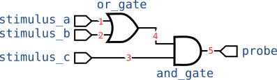
To try out our new application kernels we’ll now put together a proof-of-concept host application which uses our kernels to simulate a single circuit and hard-codes all configuration data for each application kernel. Our proof-of-concept system will simulate the following circuit:
To do this we’ll need 6 SpiNNaker cores (one for each gate, probe and stimulus). We’ll arbitrarily use the following assignment of cores:
| Component | Chip | Core | Kernel |
|---|---|---|---|
stimulus_a |
(0, 0) | 1 | stimulus |
stimulus_b |
(0, 0) | 2 | stimulus |
stimulus_c |
(0, 0) | 3 | stimulus |
or_gate |
(1, 0) | 1 | gate |
and_gate |
(1, 0) | 2 | gate |
probe |
(1, 1) | 1 | probe |
The five wires numbered 1 to 5 in the circuit diagram will be carried by multicast routes whose key is the wire number.
This assignment is illustrated in the figure below:
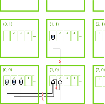
Note
Core 0 every SpiNNaker chip (not shown in the figure above) is always used by the ‘monitor process’ (SC&MP) which is used to facilitate control of the system. It cannot be used to run SpiNNaker application kernels.
We’ll run our simulation for 64 ms and configure each stimulus kernel such that each of the 8 combinations of stimulus value are held for 8 ms each to allow time for the signals to propagate through the circuit.
The proof-of-concept host program is provided in full in
circuit_simulator_proof.py and we’ll walk through the key steps below. After
creating a MachineController instance and
booting the machine as usual, the first step is to allocate memory for the
configuration structs of each of the six applications using
sdram_alloc_as_filelike():
with mc.application():
    # Allocate a tagged block of SDRAM to hold the configuration struct for
    # each application kernel.
    with mc(x=0, y=0):
        # Space for sim_length, output_key and space for 64 ms of stimulus
        # data.
        stimulus_a_config = mc.sdram_alloc_as_filelike(4 + 4 + 8, tag=1)
        stimulus_b_config = mc.sdram_alloc_as_filelike(4 + 4 + 8, tag=2)
        stimulus_c_config = mc.sdram_alloc_as_filelike(4 + 4 + 8, tag=3)

    with mc(x=1, y=0):
        # Space for all 5 uint32_t values in the config struct
        or_gate_config = mc.sdram_alloc_as_filelike(5 * 4, tag=1)
        and_gate_config = mc.sdram_alloc_as_filelike(5 * 4, tag=2)

    # Space for sim_length, input_key and space for 64 ms of stimulus data.
    probe_config = mc.sdram_alloc_as_filelike(4 + 4 + 8, x=1, y=1, tag=1)
Tip
In the code above, MachineController is
used as a context manager. This allows a common set of arguments to be
specified once, the chip coordinate arguments in this example, and omitted
in subsequent calls.
Next we write the configuration structs using Python’s struct module
and the bitarray package to
pack the desired data:
    # The stimulus data (tries every combination of a, b and c for 8 ms each)
    #         |       |       |       |       |       |       |       |       |
    stim_a = "0000000011111111000000001111111100000000111111110000000011111111"
    stim_b = "0000000000000000111111111111111100000000000000001111111111111111"
    stim_c = "0000000000000000000000000000000011111111111111111111111111111111"

    # Write stimulus configuration structs
    stimulus_a_config.write(struct.pack("<II", 64, 0x00000001))
    stimulus_a_config.write(bitarray(stim_a, endian="little").tobytes())

    stimulus_b_config.write(struct.pack("<II", 64, 0x00000002))
    stimulus_b_config.write(bitarray(stim_b, endian="little").tobytes())

    stimulus_c_config.write(struct.pack("<II", 64, 0x00000003))
    stimulus_c_config.write(bitarray(stim_c, endian="little").tobytes())

    # Write gate configuration structs, setting the look-up-tables to implement
    # the two gates' respective functions.
    or_gate_config.write(struct.pack("<5I",
                                     64,          # sim_length
                                     0x00000001,  # input_a_key
                                     0x00000002,  # input_b_key
                                     0x00000004,  # output_key
                                     0b1110))     # lut (OR)
    and_gate_config.write(struct.pack("<5I",
                                      64,          # sim_length
                                      0x00000004,  # input_a_key
                                      0x00000003,  # input_b_key
                                      0x00000005,  # output_key
                                      0b1000))     # lut (AND)

    # Write the probe's configuration struct (note this doesn't write to the
    # buffer used to store recorded values).
    probe_config.write(struct.pack("<II", 64, 0x00000005))
In order to route the multicast packets to their appropriate destinations we
must define some routing table entries on the chips we’re using. We build up a
dictionary which contains a list of
RoutingTableEntry tuples for each SpiNNaker chip
where routing table entries must be added. A
RoutingTableEntry tuple corresponds directly to
a SpiNNaker routing table entry which routes packets to the supplied
set of Routes when they match the
supplied key and mask value.
The routing tables described are finally loaded onto their respective chips
using the load_routing_tables()
method of the MachineController.
Note
The details of SpiNNaker’s multicast router are outside of the scope of this tutorial. In the next part of the tutorial we’ll use Rig’s place-and-route facilities to generate these tables automatically so understanding how SpiNNaker’s router works is not strictly necessary (though often helpful!).
In brief: we must add a routing entry wherever a packet enters the network,
changes direction or leaves the network for a local core. A packet’s
routing key is matched by an entry in the table whenever (packet_key &
table_entry_mask) == table_entry_key. If no routing entry matches a
packet’s key, the packet is ‘default-routed’ in a straight line to the
opposite link to the one it arrived on. The Section 10.4 (page 39) of the
SpiNNaker Datasheet
provides a good introduction to SpiNNaker’s multicast router and routing
tables.
    # Define routing tables for each chip
    routing_tables = {(0, 0): [],
                      (1, 0): [],
                      (1, 1): []}

    # Wire 1
    routing_tables[(0, 0)].append(
        RoutingTableEntry({Routes.east}, 0x00000001, 0xFFFFFFFF))
    routing_tables[(1, 0)].append(
        RoutingTableEntry({Routes.core_1}, 0x00000001, 0xFFFFFFFF))

    # Wire 2
    routing_tables[(0, 0)].append(
        RoutingTableEntry({Routes.east}, 0x00000002, 0xFFFFFFFF))
    routing_tables[(1, 0)].append(
        RoutingTableEntry({Routes.core_1}, 0x00000002, 0xFFFFFFFF))

    # Wire 3
    routing_tables[(0, 0)].append(
        RoutingTableEntry({Routes.east}, 0x00000003, 0xFFFFFFFF))
    routing_tables[(1, 0)].append(
        RoutingTableEntry({Routes.core_2}, 0x00000003, 0xFFFFFFFF))

    # Wire 4
    routing_tables[(1, 0)].append(
        RoutingTableEntry({Routes.core_2}, 0x00000004, 0xFFFFFFFF))

    # Wire 5
    routing_tables[(1, 0)].append(
        RoutingTableEntry({Routes.north}, 0x00000005, 0xFFFFFFFF))
    routing_tables[(1, 1)].append(
        RoutingTableEntry({Routes.core_1}, 0x00000005, 0xFFFFFFFF))

    # Allocate and load the above routing entries onto their respective chips
    mc.load_routing_tables(routing_tables)
We’re finally ready to load our application kernels onto their respective chips
and cores using load_application():
    mc.load_application({
        "stimulus.aplx": {(0, 0): {1, 2, 3}},
        "gate.aplx": {(1, 0): {1, 2}},
        "probe.aplx": {(1, 1): {1}},
    })
Note
load_application() uses an
efficient flood-fill mechanism to applications onto several chips and cores
simultaneously.
The ‘Spin1 API’ used to write the application kernels causes our kernels to
wait at the ‘sync0’ barrier once the spin1_start() function is called at
the end of c_main(). We will use
wait_for_cores_to_reach_state()
to wait for all six application kernels to reach the ‘sync0’ barrier:
mc.wait_for_cores_to_reach_state("sync0", 6)
Next we send the ‘sync0’ signal using
send_signal(). This starts our
application kernels running. After 64 ms all of the applications
should terminate and we wait for them to exit using
wait_for_cores_to_reach_state().
    mc.send_signal("sync0")
    time.sleep(0.064)  # 64 ms
    mc.wait_for_cores_to_reach_state("exit", 6)
Next we retrieve the result data recorded by the probe:
    probe_recording = bitarray(endian="little")
    probe_recording.frombytes(probe_config.read(8))
Note
Note that the probe_config file-like object’s read pointer was moved
to the start of the recording array when the configuration data before
it was written earlier in the host program.
The stimulus and recorded data are plotted using
pyplot to produce a figure like the one below:
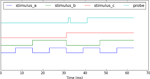
Note
The recording shows a ‘glitch’ at time=32 which is caused by propagation delays in our circuit rather than a bug in our simulator. In fact, our simulator has accurately modelled an unintended feature of our circuit!
And there we have it: a real digital circuit simulation running on SpiNNaker! Unfortunately, our simulator is not especially flexible. Changing the circuit requires re-writing swathes of code and hand-generating yet more routing tables. In the next part of the tutorial we’ll make use of the automatic place-and-route features included in the Rig library to take care of this for us. So without further delay, let’s proceed to part 05!